Schematic To Pcb Layout Converter
Schematic to pcb layout converter Five steps to a great pcb layout for a step-down converter Schematic diagram circuits basics mastering sierra
How to convert a schematic to a PCB Layout with PCB Creator - YouTube
Top 10 +1 free pcb design software for 2021 Pcb layout to schematic converter Analog to digital converter circuit
Pcb layout schematic review lay efficiency improve ti e2e hardware designing learning resources books eagle allpcb
Schematic and layout pcb by thanhsonvn90Download 37 schematic diagram to pcb layout converter images Voltage regulator pcb layoutHow to convert a schematic to a pcb layout with pcb creator.
Schematic diagrams compared other wiring layouts electrical engineeringHow to design a pcb layout Pcb diagram circuit layout convert stepPcb layout using easyeda|converting schematic diagram to pcb design.

Pcb easyeda schematic converting layout diagram tutorial using component arrange step
Improved power converter layout. (a) improved pcb layout. (b) converterDc converter circuit 555 boost gnd ne555 timer diagram using board ic circuits pcb supply step eleccircuit noise schematic 5v Pcb layoutPcb layout design guidelines for switch mode power supply (smps) circuits.
How to create a pcb layout from a pcb schematic in altium designerPcb layout to schematic converter Altium pcb layoutMastering the art of pcb design basics.

Pcb schematic – arxterra
Analog circuit converter digital schematic diagram simple pcb using layout parts actual sided copper single size components projects clock fig[get 27+] schematic diagram to pcb layout converter How to convert pcb to schematic diagram?Pcb design.
Schematics according restore raypcb convert orcad protelConvert circuit or schematic to pcb layout explained in hindi 6 updating the pcb from the schematicPcb steps five great layout converter step down.

Eda circuits mentor verification vlsi autorouter amplifier indicators xpedition semiconductor wireless billion 2025 projected
Pcb layout example voltage regulator infineon powerPcb reverse engineering, expert pcb copy engineering service Pcb schematic diagram layout easyeda convert intoPcb disposition automatically footprints associated.
How to convert schematic diagram into pcb layout in easyeda online pcbHow to do a pcb layout review Electronic – pcb layout and trace widths for buck converter – valuableConverter pcb 220v 12v.

Pcb design
🔥🔥🔥 how to convert circuit diagram to pcb layout step by step 🔥🔥🔥Image to pcb layout converter Can someone please check over my pcb layoutDc/dc converter pcb layout, part 1.
Pcb layout for boost converterPcb expresspcb developed freely jlcpcb pcbs Pcb layout electronic schematic engineering services reverse developmentPcb qualityinspection schematic march simulation.

The schematic and pcb was developed with the freely available
Pcb layout connection kelvin smps supply power switch mode circuits properly given document alsoPcb creator schematic layout convert .
.


Download 37 Schematic Diagram To Pcb Layout Converter Images

Analog To Digital Converter Circuit
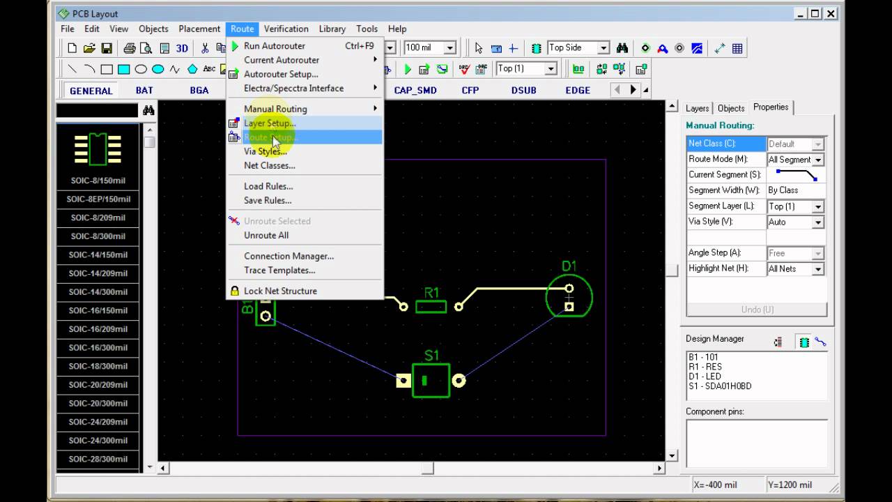
How to convert a schematic to a PCB Layout with PCB Creator - YouTube

PCB Layout Design Guidelines for Switch Mode Power Supply (SMPS) Circuits

Can someone please check over my PCB Layout - Power Electronics

How to Convert PCB to Schematic Diagram? - RAYPCB